
Micron Doubles NAND Density for 2027 Chips
The G11 generation promises faster speeds and lower power usage for AI and data center storage.
By Rebecca Kaminski ·
Data center managers and high-performance PC users will see larger storage capacities in smaller physical footprints when Micron’s G11 NAND flash arrives in the second half of 2027. The new generation doubles the storage density of current technology while cutting the energy required to transfer data.
Micron’s G11 chips will increase density from 21 Gb/mm2 to 42 Gb/mm2 in triple-level-cell form. This jump outpaces the next-generation products planned by competitors Kioxia and Samsung.
The technology also boosts input and output speeds by up to 50 percent. Data transfer rates will rise from 3,600 MT/s to 5,400 MT/s. Additionally, the energy cost to move each bit of information will drop by more than 25 percent.
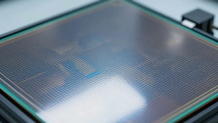
Micron adopts wafer-on-wafer bonding to build these chips. The company manufactures the memory array and the peripheral circuitry on separate wafers before bonding them together. This method allows engineers to optimize the memory and logic components independently for better performance.
Scott DeBoer, Micron’s president and chief technology and products officer, confirmed the use of this bonding technology. He stated that the timing is right for the technology to meet current product specifications and cost requirements.
The G11 design will exceed 400 layers, although Micron has not disclosed the exact count. The company attributes the density gains to a combination of added layers and smaller memory cell dimensions. More technical details are expected closer to the start of high-volume production in 2027.
Beyond G11, Micron plans to continue scaling in all three dimensions. The company is developing new high-mobility materials and ultra-dense cell architectures to improve transistor characteristics and reduce power consumption further.
Source: Tom's Hardware